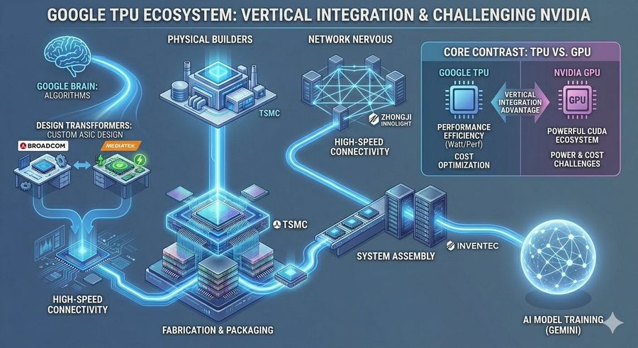
Google Tpu Ecosystem Infographic
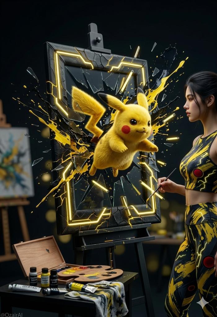
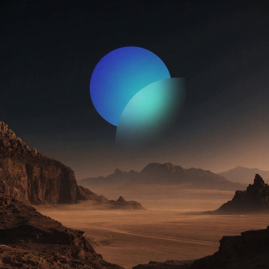
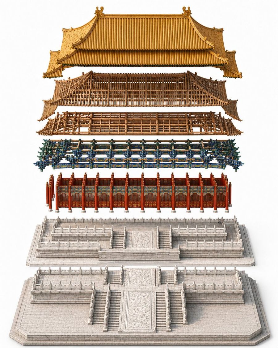
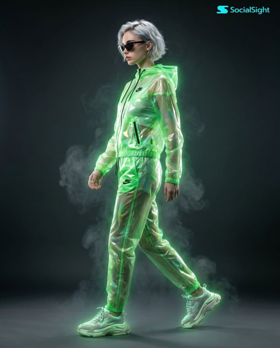
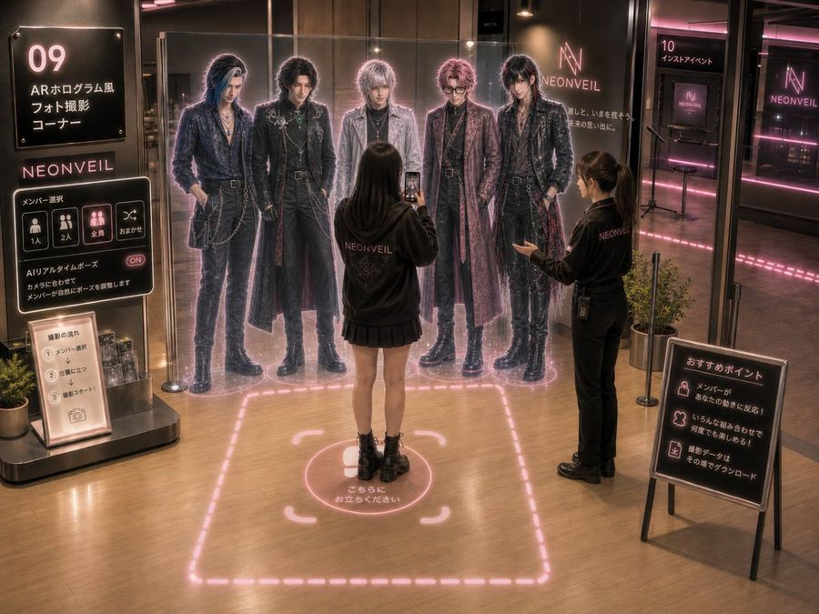
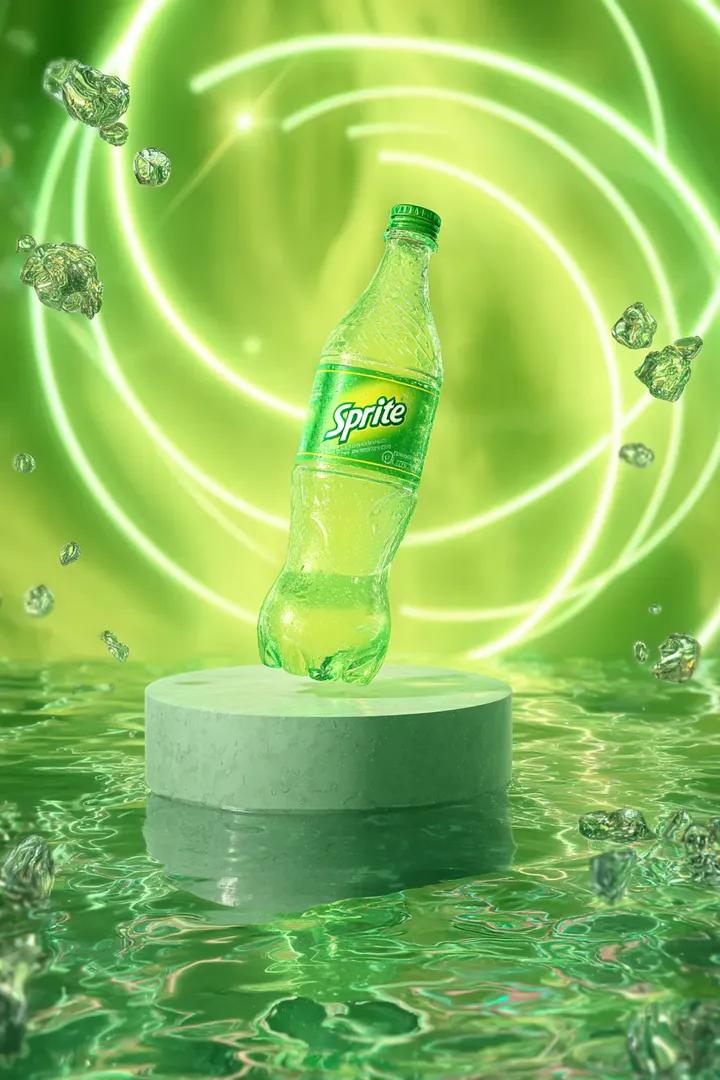
What this prompt does: Produces a 3d figurines image using GPT Image 2. Style cues: dark, ethereal, neon, isometric. Sourced from a verified fair-citation repository (铁牛) and reproduced here unchanged with full attribution per the source license.
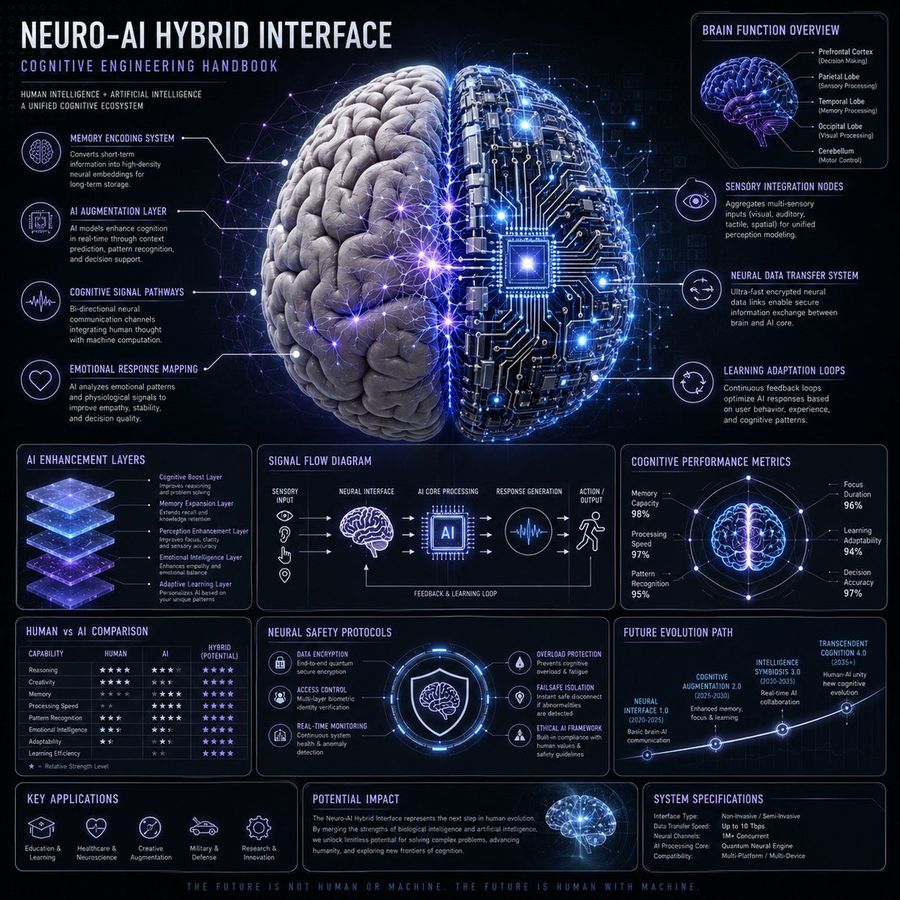
{"type":"wide futuristic tech industry infographic","title":"{argument name=\"headline text\" default=\"GOOGLE TPU ECOSYSTEM: VERTICAL INTEGRATION & CHALLENGING NVIDIA\"}","style":"dark blue isometric vector infographic, glowing cyan circuit pathways, neon highlights, 3D chip and data-center icons, clean corporate technology presentation, high contrast white uppercase labels with subtle drop shadows, 16:9 landscape","layout":{"background":"blue-gray gradient with faint circuitry, all nodes connected by luminous cyan data-flow lines","main_flow":"a left-to-right ecosystem map showing Google's TPU supply chain from algorithms and ASIC design through fabrication, networking, system assembly, and AI model training","discrete_labeled_sections_count":8,"sections":[{"title":"GOOGLE BRAIN: ALGORITHMS","position":"upper left","visual":"glowing outline brain icon feeding a cyan stream into the ecosystem"},{"title":"DESIGN TRANSFORMERS: CUSTOM ASIC DESIGN","position":"left middle","count":2,"labels":["BROADCOM","MEDIATEK"],"visual":"two small chip-design workstation tables connected by arrows, Broadcom on the left and MediaTek on the right"},{"title":"HIGH-SPEED CONNECTIVITY","position":"lower left","visual":"circuit-board routing and glowing data links feeding into the central TPU package"},{"title":"PHYSICAL BUILDERS","position":"top center","count":1,"labels":["TSMC"],"visual":"isometric semiconductor factory with a bright blue roof core, connected vertically to the central chip"},{"title":"FABRICATION & PACKAGING","position":"bottom center","count":1,"labels":["TSMC"],"visual":"large central stacked TPU chip package on a circuit substrate, glowing cyan processor die, multilayer packaging blocks"},{"title":"NETWORK NERVOUS","position":"upper center-right","count":1,"labels":["ZHONGJI INNOLIGHT"],"visual":"cluster of server towers connected by a luminous mesh network, data stream flowing downward"},{"title":"SYSTEM ASSEMBLY","position":"right center","count":1,"labels":["INVENTEC"],"visual":"rack servers and a long assembly module connected to the main TPU flow"},{"title":"AI MODEL TRAINING (GEMINI)","position":"lower right","visual":"large glowing wireframe sphere with connected nodes representing AI training output"}]},"comparison_panel":{"title":"CORE CONTRAST: TPU VS. GPU","position":"upper right","panel_style":"rounded rectangle card split vertically, cyan Google TPU side on left and purple Nvidia GPU side on right","columns_count":2,"columns":[{"heading":"GOOGLE TPU","icon":"cyan processor icon","points_count":3,"points":["PERFORMANCE EFFICIENCY (Watt/Perf)","COST OPTIMIZATION","VERTICAL INTEGRATION ADVANTAGE"]},{"heading":"NVIDIA GPU","icon":"purple chip icon labeled GPU","points_count":3,"points":["POWERFUL CUDA ECOSYSTEM","POWER & COST CHALLENGES","VERTICAL INTEGRATION ADVANTAGE shown as a central arrow contrast marker"]}]},"visual_elements":{"company_labels_count":5,"company_labels":["BROADCOM","MEDIATEK","TSMC","ZHONGJI INNOLIGHT","INVENTEC"],"major_icons_count":9,"major_icons":["brain","two ASIC design workstations","semiconductor factory","central packaged TPU chip","network server mesh","assembly rack servers","comparison card","GPU chip","AI training globe"]},"customization":"Keep all text legible and in English, preserve the exact uppercase labels, use a polished financial research infographic look suitable for explaining the TPU industry chain. Emphasize {argument name=\"highlight theme\" default=\"vertical integration and challenging NVIDIA\"} with bright cyan data paths and a premium technology aesthetic."}


![Stylized Illustration of [PRODUCT / TECHNOLOGY] Visualized — Nano Banana Pro image prompt example](https://pub-c5e3d660d0a241c5895facb8ff762e97.r2.dev/media/youmind/nano-banana-pro-8777.jpg)
![Neon X-Ray Photorealistic [OBJECT] Shown as Glowing X-ray Scan — Nano Banana Pro image prompt example](https://pub-c5e3d660d0a241c5895facb8ff762e97.r2.dev/media/youmind/nano-banana-pro-9893.jpg)